
Full hardware board is manufactured and tested
Before finalizing the next hardware revision of the OpenEPT project, several unexpected issues appeared during bring-up and early testing. None of them were critical, but each problem offered a useful lesson about component availability, schematic assumptions, and layout verification. In this short development blog I describe the most important fixes and the experience gained along the way. The goal is to help anyone working on similar hardware avoid the same pitfalls.
Oscillator
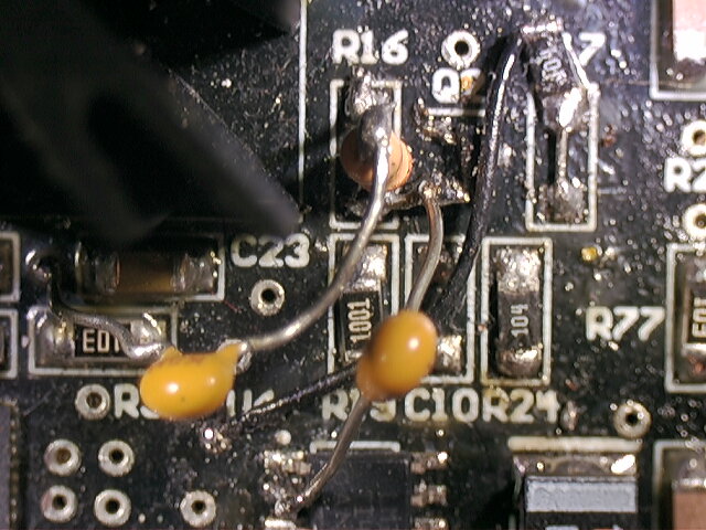
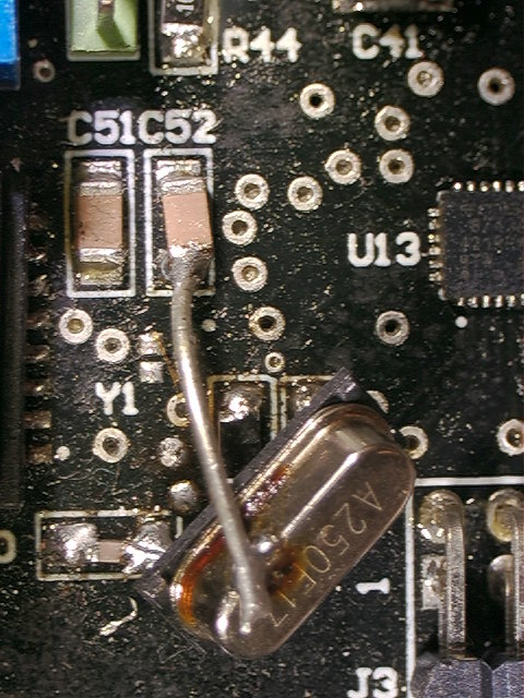
One of the first obstacles was related to component availability. The planned component, the SMD crystal oscillator NX2016SA-25.000M-STD-CZS-1, was out of stock at the moment of procurement. Since compact 25 MHz SMD oscillators are not widely available, hardware validation could not begin as intended. As a temporary solution, a through-hole HC49/U-S 25 MHz crystal oscillator was installed. This allowed testing and verification of the prototype without changing the rest of the design.
LAN Chip
A more serious issue was discovered in the LAN controller section. The LAN8742A-CZ-TR requires its internal regulator pin, VDDCR (pin 6), to be connected to ground through two decoupling capacitors of 1 µF and 470 pF. In the schematic this pin was mistakenly connected directly to the 3.3 V rail. The fix required cutting the trace between pin 6 and VDD, then routing the pin to the correct capacitor network referenced to ground. After the correction, the LAN controller worked as expected.

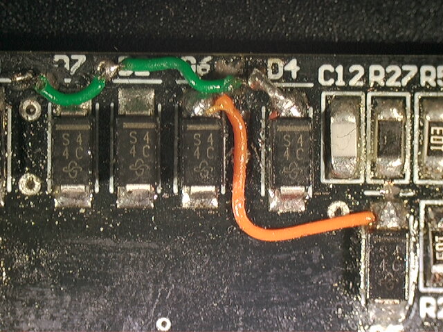
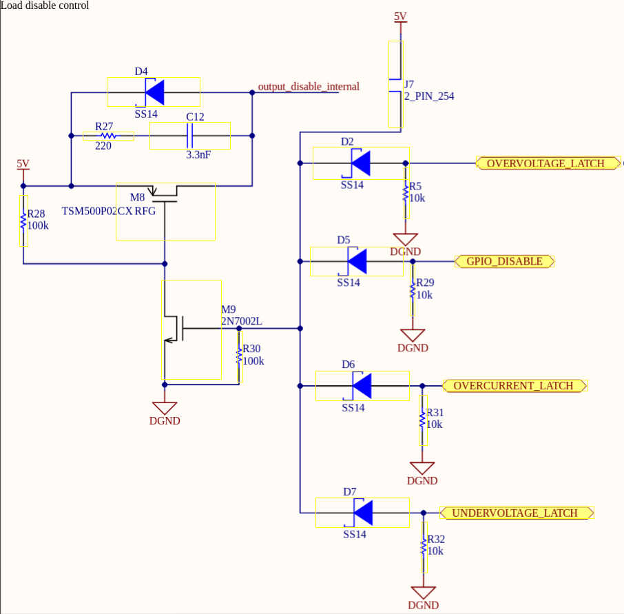
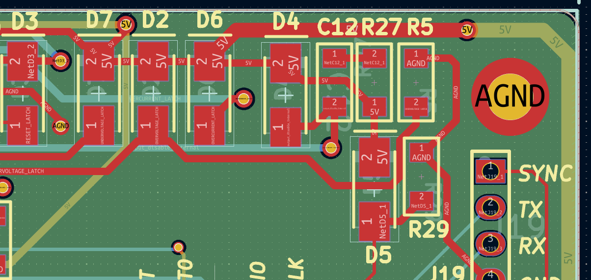
Load Disable Control
A missing jumper in the schematic, introduced during migration between CAD tools, led to a more complex issue in the PCB layout. Because the omission propagated into the board, the LOAD_DISABLE signal was permanently active. Several 5 V traces branched from the cathodes of diodes D2, D5, D6 and D7, forcing the signal high. To restore normal operation, each of these traces had to be manually cut on the PCB. This example shows how a small schematic error can quickly turn into a time-consuming physical fix.
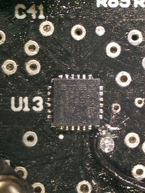
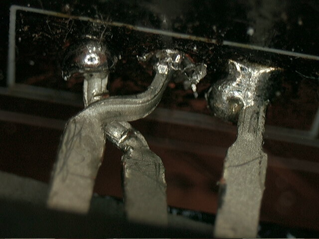
Transistor Footprint
The footprint of the main power transistor was defined incorrectly, which caused its pins to misalign with the PCB pads. The immediate workaround was to rotate the component during assembly. Although the fix was simple, identifying the source of the issue required careful inspection. This highlights the importance of verifying footprints just as thoroughly as schematics.
Op Amp Compensation Optimization
This hardware revision also includes an improved compensation network for the operational amplifier that drives the power transistor. Although not a correction of an error, the updated network provides better loop stability and improved transient response. A more detailed explanation together with simulation data and measurement results will be included in the next hardware revision.